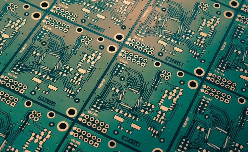
A Printed Circuit Board (PCB) is a foundational component in modern electronics, consisting of a flat board made from insulating materials like fiberglass or plastic, with conductive pathways etched from copper foil. These pathways, known as traces, connect various electronic components such as resistors, capacitors, and integrated circuits, forming a structured network for electrical signals to flow. PCBs are typically manufactured through processes like etching, drilling, and soldering, allowing for compact and reliable circuit designs. They come in single-layer, double-layer, or multi-layer configurations, enabling complex functionalities in devices ranging from smartphones and computers to automotive systems and medical equipment. By providing a stable platform for component mounting and interconnection, PCBs enhance efficiency, reduce wiring errors, and facilitate mass production in the electronics industry.
Table of Contents
- Part 1: OnlineExamMaker AI Quiz Maker – Make A Free Quiz in Minutes
- Part 2: 20 Printed Circuit Board Quiz Questions & Answers
- Part 3: Save Time and Energy: Generate Quiz Questions with AI Technology
Part 1: OnlineExamMaker AI Quiz Maker – Make A Free Quiz in Minutes
Still spend a lot of time in editing questions for your next Printed Circuit Board assessment? OnlineExamMaker is an AI quiz maker that leverages artificial intelligence to help users create quizzes, tests, and assessments quickly and efficiently. You can start by inputting a topic or specific details into the OnlineExamMaker AI Question Generator, and the AI will generate a set of questions almost instantly. It also offers the option to include answer explanations, which can be short or detailed, helping learners understand their mistakes.
What you may like:
● Automatic grading and insightful reports. Real-time results and interactive feedback for quiz-takers.
● The exams are automatically graded with the results instantly, so that teachers can save time and effort in grading.
● LockDown Browser to restrict browser activity during quizzes to prevent students searching answers on search engines or other software.
● Create certificates with personalized company logo, certificate title, description, date, candidate’s name, marks and signature.
Automatically generate questions using AI
Part 2: 20 Printed Circuit Board Quiz Questions & Answers
or
1. What is a Printed Circuit Board (PCB)?
A) A type of software for circuit design
B) A board that mechanically supports and electrically connects electronic components
C) A battery used in electronic devices
D) A microprocessor chip
Answer: B
Explanation: A PCB provides a platform for mounting components and creating electrical connections through conductive traces, making it essential for assembling electronic circuits.
2. Which material is commonly used as the base substrate in PCBs?
A) Metal alloys
B) Fiberglass reinforced epoxy resin (FR-4)
C) Rubber
D) Wood
Answer: B
Explanation: FR-4 is a standard material due to its excellent electrical insulation, mechanical strength, and heat resistance properties.
3. What is the primary function of copper traces on a PCB?
A) To provide structural support
B) To conduct electrical signals between components
C) To insulate the board
D) To add decorative elements
Answer: B
Explanation: Copper traces form the pathways that carry electrical current, enabling communication and power distribution among components.
4. Which process is used to remove unwanted copper from a PCB during manufacturing?
A) Soldering
B) Etching
C) Lamination
D) Drilling
Answer: B
Explanation: Etching uses chemicals to dissolve excess copper, leaving only the desired circuit patterns on the board.
5. What does a via do in a multi-layer PCB?
A) Connects layers electrically
B) Stores data
C) Provides power
D) Insulates components
Answer: A
Explanation: Vias are plated holes that allow electrical connections between different layers of the PCB, facilitating complex designs.
6. Which type of PCB has components on both sides?
A) Single-sided PCB
B) Double-sided PCB
C) Multi-layer PCB
D) Flexible PCB
Answer: B
Explanation: Double-sided PCBs allow for more components and denser circuitry by utilizing both surfaces for mounting and tracing.
7. What is the purpose of solder mask on a PCB?
A) To conduct electricity
B) To protect traces from oxidation and shorts
C) To add weight to the board
D) To display information
Answer: B
Explanation: Solder mask is a protective coating that prevents solder from bridging between traces and protects against environmental damage.
8. In PCB design, what does SMD stand for?
A) Surface Mount Device
B) Soldered Metal Design
C) Single Module Device
D) Standard Mounting Diagram
Answer: A
Explanation: SMD components are mounted directly onto the surface of the PCB, allowing for smaller and more efficient designs.
9. Which factor primarily determines the impedance of a PCB trace?
A) The color of the board
B) The width, thickness, and distance from the ground plane
C) The number of components
D) The board’s weight
Answer: B
Explanation: Trace impedance is controlled by physical dimensions and the dielectric properties of the substrate, which affect signal integrity.
10. What is the role of a ground plane in a PCB?
A) To generate power
B) To provide a common return path for currents and reduce noise
C) To store energy
D) To connect to the internet
Answer: B
Explanation: A ground plane helps minimize electromagnetic interference and ensures stable electrical performance by acting as a reference point.
11. Which soldering method is commonly used for mass production of PCBs?
A) Hand soldering
B) Reflow soldering
C) Wave soldering
D) Both B and C
Answer: D
Explanation: Reflow and wave soldering are automated processes that efficiently attach components to PCBs in large quantities.
12. What causes a PCB to be classified as rigid?
A) It uses flexible materials
B) It is made from inflexible substrates like FR-4
C) It has no layers
D) It is always single-sided
Answer: B
Explanation: Rigid PCBs maintain a fixed shape due to the use of stiff materials, making them suitable for standard electronic devices.
13. In PCB terminology, what is a pad?
A) A connection point for components
B) A protective layer
C) A type of wire
D) A drill hole
Answer: A
Explanation: Pads are exposed metal areas on the PCB where components are soldered, ensuring secure electrical connections.
14. Which standard is often used for PCB design files?
A) Gerber format
B) JPEG format
C) PDF format
D) Word format
Answer: A
Explanation: Gerber files are the industry standard for describing the PCB layout, including layers and drill data, for manufacturing.
15. What is thermal relief in PCB design?
A) A way to cool the board
B) Pads designed to ease soldering by reducing heat dissipation
C) A type of insulation
D) A power source
Answer: B
Explanation: Thermal relief connects pads to ground planes with narrow traces to prevent rapid heat loss during soldering.
16. Which layer of a PCB is typically used for routing signals?
A) Solder mask layer
B) Signal layer
C) Silkscreen layer
D) Ground layer
Answer: B
Explanation: Signal layers contain the copper traces that carry electrical signals between components.
17. What is the minimum number of layers in a multi-layer PCB?
A) 1
B) 2
C) 4
D) It varies, but typically more than 2
Answer: D
Explanation: Multi-layer PCBs generally have at least four layers, but the term applies to any board with more than two conductive layers for complex circuits.
18. Why is conformal coating applied to PCBs?
A) To make the board flexible
B) To protect against moisture, dust, and chemicals
C) To increase conductivity
D) To add color
Answer: B
Explanation: Conformal coating forms a protective barrier that enhances the durability and longevity of the PCB in harsh environments.
19. What does PCB prototyping involve?
A) Final production only
B) Testing and iterating designs before full manufacturing
C) Recycling old boards
D) Painting the board
Answer: B
Explanation: Prototyping allows designers to verify functionality, make adjustments, and avoid errors in the final production run.
20. Which component is essential for through-hole technology in PCBs?
A) Surface mount resistors
B) Plated through-holes
C) Flexible traces
D) LED lights
Answer: B
Explanation: Plated through-holes enable components to be mounted by inserting leads through the board and soldering on the opposite side.
or
Part 3: Save Time and Energy: Generate Quiz Questions with AI Technology
Automatically generate questions using AI